Hi @fishbone,
@robotbuilder has provided some useful annotations, and whilst I was preparing this reply, @inst-tech has provided a simulation, which hopefully will have answered your question, but just in case, I hope no-one will mind if I gild the lily, by amplifying the explanations a little more.
NB This is quite long and complex, so it is easy for a mistake to slip in ... please query anything that doesn't make sense ... it may well be my fingers hit the wrong keys!
--------------
I should like to start by pointing out something that maybe obvious, but I always feel it is safer to be sure.
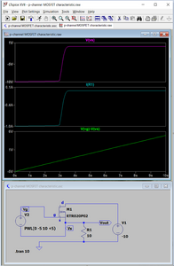
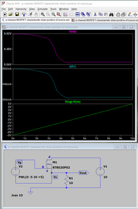
I have done a simple simulation of a convenient p-channel MOSFET with power (in terms of drain-source voltage) the 'normal' way round and 'inverted'.
The first is 'normal' in which the intrinsic diode is reverse biased:
---
The second is 'inverted' in which the intrinsic diode is forward biased, so that the FET conducts with all values of gate to source voltage. However, for a range of gate-to-source voltages, the voltage drop across the device may be less than when only the diode is conducting.
The MOSFET on this ESP32 card is connected in the 'inverted' configuration when considering powered ONLY from VBAT.
-----------
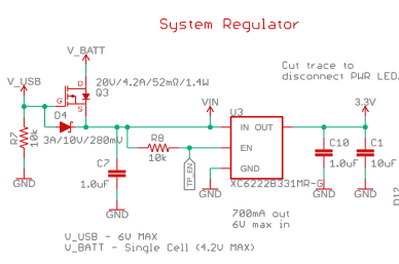
When trying to understand a new circuit, it is always useful to look around for other clues. In this case, with the help of Google, I found a somewhat similar circuit from Sparkfun at
https://cdn.sparkfun.com/assets/5/9/7/4/1/SparkFun_Thing_Plus_ESP32-WROOM_C_schematic2.pdf
which includes this snip:
And also checked on the data sheet for the voltage regulator type that I wasn't familiar with, by looking at the data sheet at https://product.torexsemi.com/system/files/series/xc6222.pdf
and the MOSFET data sheet at
------------------------------------------
The Sparkfun schematic provided some text:
V_USB : 6V max
V_BATT : Single Cell (4.2V max)
(and I used the voltage regulator reference to find the data sheet)
---
The voltage regulator data sheet said it had:
(worst case) max dropout voltage of 0.2 V, and the regulated output voltage was 3.3V, implying that it could maintain 3.3 V output for input voltages down to (3.3 + 0.2) = 3.5 V. Also that the maximum acceptable input voltage was 6V.
---
The MOSFET data sheet said it was a P-Channel 20-V(D-S) MOSFET, with a typical body diode drop of 1.2V at 0.7 A and a maximum drop of 1.2V at 0.7 A current. Typical drain-source resistance with gate-source voltage of -2.5V, is 0.11 Ohm.
---
Although I could have guessed values for VBAT etc., these extra points give me a better idea of what voltages the dev board was expected to be operating with.
------------------------------------------------------------------------------
There are three possible power inputs. Initially assume only one source at a time is active, assemble a series of preliminary observations as CLUEs, by considering the different facts and options.
---------------------------------------------------------------------------
CLUE A: Working voltage range at input to voltage regulator : 3.5 V to 6V (from regulator data sheet)
-------------
CLUE B: When powered via the Board pin VIN, CLUE A applies : 3.5 V to 6V (from schematic)
--------------
When powered via VBAT:
Maximum expected battery voltage is 4.2 V (From Sparkfun schematic comment)
Power will initially be conducted through the intrinsic diode of the FET (from schematic + knowledge of MOSFET characteristics). Typical voltage drop across the diode may be around 0.7V, resulting in the voltage at the drain of the MOSFET being about 3 V, whilst the gate is held at 0V by the resistor. This means Vgs is -3V, which will cause it to conduct, and this will further reduce the voltage drop across the FET and increase the voltage arriving at the input of the voltage regulator.
CLUE C: When powered via VBAT, the intrinsic diode will initially conduct the power from the battery to the input of the voltage regulator, and this will cause the FET to conduct, enhancing the power flow to the voltage regulator.
----------
When powered by VBUS:
The circuit between the USB socket and VBUS is not shown, so for simplicity, assume it is wired directly.
The incoming USB voltage should be close to 5V. This will be conducted with a single diode D1 voltage drop, which is likely to be in the range of 0.3V to 0.7V, depending on diode type. The result should be a voltage in the range of about 4V to 4.8V at the input of the regulator, which is comfortably in the acceptable range of 3.5V to 6V.
CLUE D: When powered by the USB socket/VBUS, the diode D1 will provide the current flow to the voltage regulator.
-------------
Hence, all 3 possible sources can provide the power to the voltage regulator. However, that is not the full picture. Simply wiring all of the possible inputs together could have achieved that, but the circuit is 'more complex' than a simple wire to provide some protection in the circumstance that two or three of the power sources are simultaneously 'active'. That is the circuit has a 'priority' system that chooses which is the 'best' to use, whilst (attempting) to ensure that one supply cannot drive power into the other supplies.
This sermon is already too long and complex, so I'll only mention some of the cases to consider ... a competent designer would diligently try to consider all possible events before releasing a design!!
---------------
VBAT and VBUS (USB) inputs both powered.
VBAT has a maximum voltage of 4.2 V, and will suffer a voltage drop passing through the FET
VBUS has a 'normal' voltage of about 5V, which will suffer a voltage drop passing through the diode D1. VBUS will also ensure the FET gate voltage is about 5V, whilst the FET source voltage will be less than 5V, ensuring the FET is in the non-conducting state.
If the VBUS voltage is lower than normally expected, resulting in the VBAT voltage to be higher than the voltage at the input to the voltage regulator, then in principle, the FET intrinsic diode can stlll conduct power from VBAT to the regulator, but in practice the voltages are likely to restrict any such current to a low value. This would result in the battery discharging. More importantly, if the voltage at the voltage regulator was higher than VBAT, then the intrinsic FET diode would be reverse biased, and the FET non conducting, so that power from VBUS could not charge the battery.
CLUE E: MOSFET allows battery to power the voltage regulator when VBUS voltage is low or missing, and prevents battery being charged by VBUS when VBAT is low compared to VBUS.
---------------
VIN and VBUS inputs both powered.
Diode D1 should prevent any current flowing back into the VBUS and the USB host. Note this only applies for voltages VIN in the range up to 6V.
NB Voltages just over 6V are likely to destroy the voltage regulator, but substantially higher voltages may also destroy the USB host, and PCs tend to be more expensive losses than an ESP32 card!!
The VIN power source has no reverse current protection, so powering both VIN and VBUS at the same time is not advisable.
CLUE F: Only power by one of VIN or VBUS, never both simultaneously.
----------------
I am sure this is much more than you expected or feared. Considering the whole discussion is based on just 1 MOSFET, 1 resistor, and 1 diode, it is not surprising you found it looked more difficult to understand than you expected it to be. I just hope that you carefully read through this and the other contributions and make sense of the picture in your own mind. Feel free to clarify any questions or problems that arise.
Best wishes and good luck with your projects, Dave
@zander Ahhh.. Thanks a lot Ron.. that's a bit better than a screen shot!
I will be using that for now on..again, appreciate all you help and advice..
Take care my friend,
regards,
LouisR
LouisR
@inst-tech Too bad you didn't know, those MOSFET circuits could be useful to lots of members. I might print your circuits out and attempt to build them in falstad. I have tried to use it before but always got stumped somewhere.
First computer 1959. Retired from my own computer company 2004.
Hardware - Expert in 1401, and 360, fairly knowledge in PC plus numerous MPU's and MCU's
Major Languages - Machine language, 360 Macro Assembler, Intel Assembler, PL/I and PL1, Pascal, Basic, C plus numerous job control and scripting languages.
Sure you can learn to be a programmer, it will take the same amount of time for me to learn to be a Doctor.
@zander , Indeed..Falstad is fairly easy to use for simple ckt., but doesn't have enough "help" to be able to figure out how to use it.. there are properties for each component that you can modify, and also create properties for new components, as I have done in the circuit we have been discussing. I just like it because it's dynamic and has that oscilloscope and trending feature so I can change values and components on the fly, and see how that affect the circuit.
There's a steep learning curve for many of the components that are not commonly used, but overall, It's much quicker than TINA, or LTspice...
Well, now that you have shown me how to export Falstad, It will be easier to show future queries that I'm trying to convey.
Be well my friend,
Regards,
LouisR
LouisR
@inst-tech I can definitly see the benefit of using falstad, but I have not been able to master it. That is proly more my issue than anything else. Some things I learn very fast, some are impossible. I am going to use your screen grabs to guide me in creating a falstad circuit. Then I can export it. I think I will add a new topic under Tools and Test Equipment called Falstad circuits IF I can get your circuit entered. Being able to show V's and A's plus scope traces is a big advantage. One of the things I am having some trouble with is arranging the scope windows and various test points meters etc. I will look for some help or tutorial today.
EDIT: I found the manual, it's at https://www.memphis.edu/et/publications/index.php (see pic) and a mini manual at https://www.falstad.com/circuit/directions.html
I will try to fit this into my learning schedule, but no promises at my age.
First computer 1959. Retired from my own computer company 2004.
Hardware - Expert in 1401, and 360, fairly knowledge in PC plus numerous MPU's and MCU's
Major Languages - Machine language, 360 Macro Assembler, Intel Assembler, PL/I and PL1, Pascal, Basic, C plus numerous job control and scripting languages.
Sure you can learn to be a programmer, it will take the same amount of time for me to learn to be a Doctor.


