@robotbuilder And exactly how do I do the following?
A small current controlling a larger current by adjusting the resistance between the collector and emitter.
First computer 1959. Retired from my own computer company 2004.
Hardware - Expert in 1401, and 360, fairly knowledge in PC plus numerous MPU's and MCU's
Major Languages - Machine language, 360 Macro Assembler, Intel Assembler, PL/I and PL1, Pascal, Basic, C plus numerous job control and scripting languages.
My personal scorecard is now 1 PC hardware fix (circa 1982), 1 open source fix (at age 82), and 2 zero day bugs in a major OS.
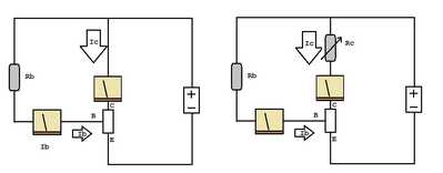
Maybe the block cct schematic will explain what I am writing about.
I actually used a uAmp meter to read the base current Ib and a mAmp to read the collector current Ic
I adjusted the base current Ib to produce a certain collector current Ic
Then I added a variable resistor Rc in the collector current path.
Note Rc and the collector to emitter are in series. If you imagine a variable resistor between C and E it would be forming a voltage divider with the resistor Rc.
In the example on the left the voltage at the C terminal will be the same as the battery voltage.
In the example on the right you can vary the collector resistor Rc.
You will observe the collector current Ic will try and remain constant because the transistor adjusts the collector current to a value BETA * Ib if physically possible. Try it with a real variable resistor (POT) instead of the transistor. When the full voltage of the battery is across the Rc resistor the variable resistor will have reduced to zero. The voltage at the collector terminal will vary between the full battery voltage and zero.
I emphasize this because it wasn't until I realized the transistor was trying to maintain this constant current determined by the base current value regardless of the value of the Rc resistor that the circuits made sense.
There is a lot more to real transistors to be considered in real circuits but that is another story.
To enlarge the image, right click the image and choose Open link in new window.
@robotbuilder I bookmarked your post, but between a new puppy and ongoing health issues, I don't have the energy to set it up (also still suffering from move-in and organizational woes).
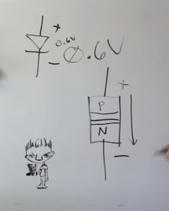
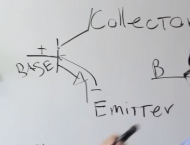
What about my other post? The presenter first shows the in the diode circuit current flowing one way (with the arrow as expected), but then when he shows the transistor circuit, he suddenly has the current flowing E to B against the arrow.
This is the Sparkfun set of videos so he isn't an amateur.
First computer 1959. Retired from my own computer company 2004.
Hardware - Expert in 1401, and 360, fairly knowledge in PC plus numerous MPU's and MCU's
Major Languages - Machine language, 360 Macro Assembler, Intel Assembler, PL/I and PL1, Pascal, Basic, C plus numerous job control and scripting languages.
My personal scorecard is now 1 PC hardware fix (circa 1982), 1 open source fix (at age 82), and 2 zero day bugs in a major OS.
@robotbuilder @davee I think I figured it out. When he is discussing the diode theory, he is using 'conventional' + to - theory which is what I was taught. In the transistor circuit he switches to the new - to + convention. I deduced that because he has the main current flowing from the emitter at ground potential to the collector at Vcc potential.
I will make sure the author knows.
Now, I am not sure why just because a small E to B current flows that a larger (100x, more) flows from E to C. Is that just the 'magic' of a doped region?
First computer 1959. Retired from my own computer company 2004.
Hardware - Expert in 1401, and 360, fairly knowledge in PC plus numerous MPU's and MCU's
Major Languages - Machine language, 360 Macro Assembler, Intel Assembler, PL/I and PL1, Pascal, Basic, C plus numerous job control and scripting languages.
My personal scorecard is now 1 PC hardware fix (circa 1982), 1 open source fix (at age 82), and 2 zero day bugs in a major OS.
It doesn't matter which way you decide the "electricity flows" as long as you are consistent. It is easier to understand if you learn about static electricity. A positive charged particle moving one way has the same effect as a negative charged particle moving the other way.
I don't understand the physics of transistors. All I know is a small source of energy is controlling a larger source of energy just as you do when you use your weak muscles to pull a lever that controls a strong hydraulic digger.
A simple "digital amplifier" could be an electro magnetic relay. A small current closes a mechanical switch that closes the path in a high current circuit. Maybe you could use a small current to drive a weak motor that turns a POT that in turn controls a larger current for a slow analog version of an amplifier.
I haven't played with analog circuits for a long time. Transistors in digital circuits operate in the extreme position of ON or OFF meaning the collector to emitter (or source to drain in a MOSFET) has a LOW resistance or a HIGH resistance. The MOSFET gate voltage controls flow between the source and drain. I imagine it like squeezing a soft hose to control the flow of water or air flowing through the hose.
Moving charged particles have a magnetic field curled around them, which you can detect with a magnetic compass. Positive charged particles moving one way produce the same magnetic North South direction as a negative charged particle moving in the opposite direction. That is how the electric current meters work. You use them to see how much electricity is flowing past a particular point by the strength of the associated magnetic field.
Electric pressure (measured in volts) is always relative, between two points. in a simple dc circuit one battery terminal is used as the reference point and all other points in the circuit have a voltage value relative to that terminal.
@robotbuilder The problem is in the YT video I found from your Sparkfun link; he uses conventional flow, which I learned in HS in the early 60s and used as an industrial electrician then as an IBM field engineer in the late 60s. I have never heard about this change in theory until very recently. Then he changed to electron flow or whatever it's called. I will re-watch the video and write down a description of what is happening using conventional flow so I can understand it. I see no reason to 'think' in terms of resistors, I have a basic understanding of the physics involved but have not used that knowledge for over 60 years, so it's a lot rusty.
First computer 1959. Retired from my own computer company 2004.
Hardware - Expert in 1401, and 360, fairly knowledge in PC plus numerous MPU's and MCU's
Major Languages - Machine language, 360 Macro Assembler, Intel Assembler, PL/I and PL1, Pascal, Basic, C plus numerous job control and scripting languages.
My personal scorecard is now 1 PC hardware fix (circa 1982), 1 open source fix (at age 82), and 2 zero day bugs in a major OS.
Hi Ron @zander,
Sorry, I don't have any 'off the shelf' sermons on NPN & PNP transistor operation. In fact, I have yet to see a 'simple' explanation as to what is going on inside, that is convincing. So this is more of a meander of what I have found to be useful.
It has taken me some time to write this, and the conversation has moved on a bit.
I will agree that either conventional current or electron current can be considered for most purposes of someone trying to understand how a circuit works. (See https://en.wikipedia.org/wiki/Electric_charge )
i.e. It is still often convenient to use 'conventional' current, which dates back to Benjamin Franklin in the 1740s, which imagines positive charges moving out from the positive terminal of a battery, through an external circuit (e.g. a light bulb) to the negative terminal, whilst the more physically accurate picture, which become apparent in the 1890s, known as 'electron current' is of negatively charged particles emanating from the negative terminal of the battery, through the external circuit, to the positive terminal of the battery.
Hence, when considering a circuit, don't worry too much about the physical reality ... just pick one 'type' of current and use it consistently for the immediate discussion.
--------------------------------------------
A quick look at the Sparkfun page
https://learn.sparkfun.com/tutorials/transistors/symbols-pins-and-construction
didn't reveal any obvious mistakes on their part ... providing you read the text, as well as looking at the pictures, but please note the text includes gems like:
Don't base your understanding of a transistor's operation on that model (and definitely don't try to replicate it on a breadboard, it won't work). There's a whole lot of weird quantum physics level stuff controlling the interactions between the three terminals.
which is probably true, but is short on explanation.
All About Circuits has a bash at explaining a model of what is happening, but whether it will really help you, I am less clear:
https://www.allaboutcircuits.com/textbook/semiconductors/chpt-2/bipolar-junction-transistors/
------
For now, I suggest that you don't try to understand what is going on inside the transistor, but treat it more like a black box with three leads, and concentrate on what is likely to happen when you wire it up in some way.
So VERY simplistically:
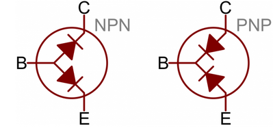
If you use an Ohm-meter to measure resistance between the transistor's leads, then obviously you can only connect to 2 of the 3 leads at any one time. And if you methodically measure the resistance between each pair of transistor leads, swapping the Ohm-meter leads to measure the 'forward' and 'backward' resistance, then it will behave the same as two diodes joined anode-to-anode if it is an NPN or cathode-to-cathode if it is a PNP, as illustrated in the Sparkfun page reference above
However, whilst this is a reasonable way of checking to see if the device has dramatically failed with a short-circuit or open-circuit junction, it tells you NOTHING about how it will work in an amplifying circuit, when all three leads are interacting.
Indeed, it suggests you should never see any current flow between the collector and the emitter, as a voltage applied from collector-to-emitter of either polarity will always encounter one of the two series connected diodes in the reverse biased situation, so no current can flow from collector to emitter. Clearly, that would not be a useful device!
----------
So I suggest you start by accepting that some 'magic' happens, when all three leads are connected to a suitable circuit, that partially contradicts your Ohm-meter's findings! That is, it is possible for a current to pass from the collector to emitter (or vice-versa, depending on whether it is NPN or PNP, and you are imagining conventional or electron current), but only when there is some base-to-emitter (or vice-versa again etc.) current, to 'unlock' the magic.
----------------------
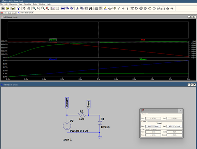
Now, I am going to start by simulating a simple silicon diode .. IN914, so we have a 'reference' to compare with. This is the diode, in series with a resistor to limit the current, connected to a voltage source that gradually increases from 0V to 2V. The diode anode is connected to the positive terminal of the supply, so that the diode is 'forward' biased, and will be expected to allow the current to flow through it. (Click on the picture to expand it.)
Note that as the voltage increases from 0V to about 350 milliVolts, the current remains almost zero, but further small increases in voltage start to dramatically increase the current. This means that the voltage across the diode (labelled V(base) for reasons that will be more apparent in the next section) becomes "almost" constant at around 400 microVolts for currents of 10 microAmps to 150 microAmps.
Furthermore, note that although the voltage across the diode is increasing, with increasing current, the higher the current, the nearer the voltage line approaches, but never achieves, a horizontal line. However, we can guess that the current might need to be (say) 100 milliAmps to reach 600 milliVolts.
The exact voltages and currents depend on the construction of the device, but this behaviour is typical of all 'normal' silicon diodes.
---------------------------
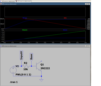
Now let's modify the circuit to use a small NPN transistor, but only connect the base and emitter, so that the internal base-emitter diode discussed near the start is forward biased.
It now becomes apparent why I named the wire conected to the anode of the diode in the first circuit V(base), as obviously it is now connected the base of the transisistor, and since the emitter is connected to the 0V line, V(base) is the same as the base-emitter voltage.
Note that although the diode and transistor were chosen as simply being the first in the list of common parts by the simulator designer, the voltage and current relationship is almost identical. So, at this point the only magic seems to be that the base-emitter junction behaves like a diode ... something the Ohm-meter suggested from the start ... so not much of a surprise!!
Note that for convenience, I am plotting the current entering the base of the transistor as I(R2), as clearly the current passing through R2 must be the same as the base current, but because of the way the simulator works, it is showing as a negative current. This is the same as measuring current with a multimeter, but accidentally connecting the leads the wrong way round. If I was producing a 'professional' sermon I would redo the slides, but for now, please compensate in your mind.
----------------------------
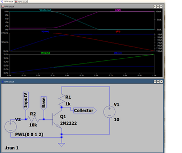
Now extend the circuit by connecting a second power source, a 10 Volt supply across the collector - emitter, using a resistor to act as a load.
The bottom two graphs are now similar to those with the transistor connected by only the base and emitter, albeit the base voltage is a little higher, and very similar to the diode simulator above, so this part of the circuit appears to have only been slightly affected by adding the collector circuitry.
But note:
- The collector current, when the base voltage is in the range 0 to 350 milliVolt, is zero, as is the base current.
- As the base voltage further increases, both the base current and the collector current start to rise. As mentioned above, please ignore the base current being shown as negative.
- As the collector current increases, the voltage drop across R1 increases, as per Ohm's Law V = IR, and hence the collector-emitter voltage decreases.
- As the base current continues to increase, when the collector current approaches 10mA, almost all of the 10V supply voltage is dropped across R1, leaving only a fraction of a volt across the collector-emitter. At this point, the transistor is said to be 'saturated' .. that is the collector current is at a maximum, the collector voltage cannot drop any lower, even though the base current can be driven to higher levels
- Compare the base and collector current levels at a convenient point in the region where both the base current and collector current are changing when the voltage applied to the input of R2 is changed ..
- e.g at 0.5 seconds, the R2 input voltage will be 1 V, base current about 30 microAmps, collector current about 3milliAmps
- So a small change of base current is making a much larger change of collector current .. maybe 10 microAmp change of base current corresponds to 1 milliAmp of collector current .. a current gain of 100 times.
------------------------------------
I think that is more than enough for now ... obviously there are lots of formulae to predict and describe what is happening, but hopefully this is enough to get a 'gut feel' as to how a bipolar transistor works. I have described an NPN transistor .. a PNP is a bit like its electrical mirror image ... it behaves in a similar way, but all of the polarities are reversed.
Note, it is quite different to its MOSFET colleagues.
-------------------
I hope this is useful. It is a 'personal and simplified' view of how to make sense of the world .. not a formal definition, and certainly not an explanation of how it achieves the magic.
But sometimes it is convenient to be like a chef --- few chefs could describe the detailed chemical reactions that convert a sticky cake mixture into sponge cake, but the good ones know how to mix the reagents in the appropriate quantities, plus how long to leave it in the oven at the temperature they selected. Furthermore, they have sufficient 'feel' of the process to be able to make a wide range of variations, each to suit the occasion.
Happy circuit baking .. best wishes, Dave
@davee @robotbuilder I don't know how I was so misunderstood. I asked why the Sparkfun YouTube video had the current going one way when discussing diodes and the other way when discussing transistors. After I asked the question, I figured out that the diode discussion was what I was taught now called 'conventional' current flow, i.e. plus to minus. I, at some point, realized (when I noticed that the emitter was connected to ground (common?) that the transistor circuit was using what is known as 'electron flow.' I am shocked that Dave said it was around since 1890. Are you sure you don't mean the 1980s? I only heard of it a few weeks ago while discussing a circuit offline and was told the electrons went out the negative battery post, and this is from a gentleman almost as old as me. That is all background.
My question was, why were two different current flows used in one video with no warning that I noticed? video here >>>
Please take a look at the pictures for the diode and transistor diagram with arrows in reverse.
I have the answer to my question, and now I need to review the video on the transistor and re-write it using 'conventional flow.' But first, I will look for a write-up, perhaps on Sparkfun, that does that for me. I was starting to gain an understanding of how solid-state devices work when I watched the diode part, but due to the unknown change in the rules, I lost the train of thought during the transistor discussion.
This is just educational for me, I do not plan on using transistors as switches, which violates my personal design beliefs when I have logic-level field effect devices that are much more similar to physical switches.
I will want to learn how to use transistors for other purposes if/when I find a need.
Thanks for your interest; I will endeavour to phrase my questions more clearly in the future to not waste everyone's time on the wrong tack.
EDIT: I did find this in the Sparkfun documentation
The NPN transistor is designed to pass electrons from the emitter to the collector (so conventional current flows from collector to emitter).
First computer 1959. Retired from my own computer company 2004.
Hardware - Expert in 1401, and 360, fairly knowledge in PC plus numerous MPU's and MCU's
Major Languages - Machine language, 360 Macro Assembler, Intel Assembler, PL/I and PL1, Pascal, Basic, C plus numerous job control and scripting languages.
My personal scorecard is now 1 PC hardware fix (circa 1982), 1 open source fix (at age 82), and 2 zero day bugs in a major OS.
Hi Ron @zander,
I had a quick look to see what Sparkfun are saying, albeit not watching the whole video, and I think he was just considering the magnitude of the current, so that he can calculate resistor values. He doesn't care whether it is conventional or electron current.
It is very common for electronic engineers to use 'conventional' current when it is convenient to do .. and not because they haven't heard about electrons. It is not a conscious choice ... it simply doesn't matter for the purpose of the analysis. That is, the circuit is already designed with appropriate voltages, so only the direction of current will be defined.
To me it is like how we buy things .. the obvious thing is 'money' .. coins, notes .. which are 'positive' value tokens.
But now, I can't remember when I last paid for something with cash ... Most of the time I use a credit card ... and that is a way of moving debt or 'negative' money around.
Both can be useful in the right circumstances, and they are effectively interchangeable.
So probably, the Sparkfun author didn't even consider which kind of current was being discussed .. it is current flow either way.
----
And no, I did mean 1890s, as per the Wikipedia reference, though I would have guessed roughly the same date, before checking. This is the period the structure of the atom, etc. started to be revealed. Because it is 'easy' to strip electrons from atoms, they were among the first to be identified and the quantisation nature of atomic particles, etc. became increasingly apparent in the early 1900s.
Wikipedia reference includes "After discovering the quantized character of charge, in 1891 George Stoney proposed the unit 'electron' for this fundamental unit of electrical charge. J. J. Thomson subsequently discovered the particle that we now call the electron in 1897. "
The fact that we have 'conventional current' has its origins back more than yet another century, when it was 'assumed' that charge would be a 'positive' thing. It is somewhat unfortunate, then when it was finally identified, it turned out to have a negative charge!
-----------
re: Now, I am not sure why just because a small E to B current flows that a larger (100x, more) flows from E to C. Is that just the 'magic' of a doped region?
Simplistically, the bipolar transistor consists of three layers sandwiched together. They are all doped, the outer layers with one type of dopant, the middle with the 'opposite' type of dopant. Furthermore, the dopant levels are all carefully adjusted, with concentration gradients, etc. to produce a device with the most desirable characteristics for a particular type of circuit. And yes, the result includes the magic that means a 'small' base-emitter current change and cause a 'larger' collector-emitter current change.
As I tried to explain, although I generally like to see the fine details, I am not sure trying to understand what happens at the subatomic level in a bipolar transistor is particularly helpful to someone designing a circuit. Obviously, if you intend to start designing and fabricating your own transistors, the situation might be different.
Best wishes, Dave
@davee, I understand both ways can be explained, but when the diode was explained using conventional, then when he did the transistor with no notification, I think you can imagine how confused I was. I understood what was happening at the diode level, and when he started to present the transistor in my head, I was already thinking this was what he would say, so when he didn't, I began to doubt my sanity.
Understanding what is happening at the sub-atomic level is very helpful for me. It's just how my brain works; I need to see the why instead of just accepting dogma.
Strangely, I don't have a problem with MOSFETs because they behave like I expect them to and are my preferred device for making a switch.
The Sparkfun article has some circuits in it, and I will breadboard them and even use my new scope to see the values using the two channels (now I wish I had 4) to see differences. I will also use my two VOMs to measure the various currents (I may have a 3rd VOM, but if I don't, I think I may get one or bite the bullet and get a precision nA meter, which I want for my low power studies in any case.)
Now I am hoping Sparkfun has an equivalent document on Fet's and tells me how to read the datasheets.
First computer 1959. Retired from my own computer company 2004.
Hardware - Expert in 1401, and 360, fairly knowledge in PC plus numerous MPU's and MCU's
Major Languages - Machine language, 360 Macro Assembler, Intel Assembler, PL/I and PL1, Pascal, Basic, C plus numerous job control and scripting languages.
My personal scorecard is now 1 PC hardware fix (circa 1982), 1 open source fix (at age 82), and 2 zero day bugs in a major OS.
Hi Ron @zander,
I think MOSFETs are more amenable to explaining how they work than BJTs, but both types have their uses.
As for scope, I presume your scope can capture traces to USB sticks, and maybe to Ethernet. That way you can do 1 measurement, record it and do the next, etc, and put the displays side by side, either on a large screen or on printouts. That is usually better than trying to get too many things set up at the same time, with scope probes unclipping themselves, etc.
A large percentage of my use is with a roving probe .. and that usually means one probe, and maybe a second clipped somewhere as a timing reference. For 4 channels I would need at least a couple of extra hands and arms .. Just a thought ...
Yes, I can imagine the Sparkfun video could be confusing. Most of what I saw was generally correct, but it jumped around quite a lot, as well as having inconsistencies. I would expect that in a 'brainstorm' meeting, but not in a teaching video.
As for low power, I would do some back of the envelope calculations to figure out how low the current needs to be. When you start going below 1 microAmp, things can get tricky, with unexpected leakage, batteries internal discharge current higher than the load, and so on. So try to figure out what is likely to be useful before buying too much supersensitive stuff.
Best wishes and take care, Dave
@davee Actually, my scope can split the display either vertically or horizontally, so seeing two is fine. It also has a facility like a VOM, so the scope is, in effect, two VOMs. The type of clip on my scope is not prone to unclipping like less expensive scopes.
Regarding low power, I plan on getting a proper nano amp meter. A standard VOM is pretty much useless below a certain point well north of where I expect to be. It is more expensive than a simple VOM but not as expensive as the scope.
First computer 1959. Retired from my own computer company 2004.
Hardware - Expert in 1401, and 360, fairly knowledge in PC plus numerous MPU's and MCU's
Major Languages - Machine language, 360 Macro Assembler, Intel Assembler, PL/I and PL1, Pascal, Basic, C plus numerous job control and scripting languages.
My personal scorecard is now 1 PC hardware fix (circa 1982), 1 open source fix (at age 82), and 2 zero day bugs in a major OS.
Understanding what is happening at the sub-atomic level is very helpful for me. It's just how my brain works; I need to see the why instead of just accepting dogma.
Ok. There are however levels of understanding.
You do not of course need to understand the physics of semi conductors to use them.
Most analog circuits (for example music, television) have gone digital. Most (all?) useful analog circuits now come in an IC package. However there are simple transistor circuits for you to build and analyse how they work. This understanding is more at the level of a mathematical analysis.
https://www.homemade-circuits.com/how-to-build-simple-transistor-circuits/
Have fun!
@robotbuilder Thanks Dave, I have bookmarked the site.
First computer 1959. Retired from my own computer company 2004.
Hardware - Expert in 1401, and 360, fairly knowledge in PC plus numerous MPU's and MCU's
Major Languages - Machine language, 360 Macro Assembler, Intel Assembler, PL/I and PL1, Pascal, Basic, C plus numerous job control and scripting languages.
My personal scorecard is now 1 PC hardware fix (circa 1982), 1 open source fix (at age 82), and 2 zero day bugs in a major OS.
@dronebot-workshop Bill, Thank you, that video was very helpful. I have a prototype working as expected now. One think I'm still trying to understand is how to calculate the value of the base resistor. Your example used an 2.2K resistor. I looked up the datasheet for the TIP121 transistor and the max base current is 120mAdc. The Arduino is supplying 5volts so the resistor needs to be 5V/.120A = 42Ohms. Nowhere need the 2.2K you used? I must be missing something.

